
 Industry Applications
 Packaging and palletizing
 Intelligent logistics and warehousing
 Digital software
 Non-standard equipment
 Integrated Circuits
 Semiconductors
 Automobile lithium battery
 Textile & film
 Universal machine
Machine Vision
2D measurement of wafer back end
Flexible and efficient multi-modality defect Re viiew and automatic defect classification.
Machine Vision
Flexible and efficient multi-modality defect Re viiew and automatic defect classification.
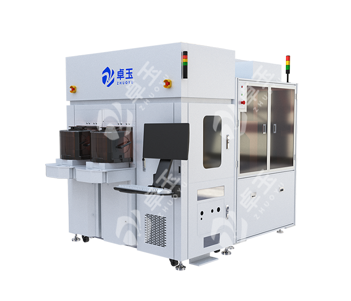
The device can automatically adjust the light intensity, switch the light source, lens, automatic optical focus, automatic optical correction, and can inspect the appearance of defects in the post-process of wafers, compatible with 8", 12" wafers. This equipment can automatically adjust the light intensity, switch the light source, lens, automatic optical focus, and automatic optical correction, and can inspect the appearance of defects in the post-process of wafers.
High-resolution optical imaging, automatic optical focus, automatic optical correction, multi-dimensional optical imaging and fast and efficient algorithmic processing capabilities.
| Model | JY-200 |
| Wafer Size Support | 200mm&300mm |
| Multiple objective switching | Multiple objective switching |
| Detection efficiency@200mm | 74WPH@2X |
| 60WPH@3.5X | |
| 37WPH@5X | |
| 10WPH@10X | |
| Color Camera | No need to review and take photos at the same magnification |
| Resolution | 4.36μm@2X |
| 2.49μm@3.5X | |
| 1.7μm@5X | |
| 0.875μm@10X | |
| 0.437μm@20X(review) | |
| Bright field lighting | High uniformity bright field lighting |
| Dark field lighting | Low angle annular dark field lighting |
| Camera | Black InspectionColor Inspection&Review |
| Large color difference wafer defect detection | Support |
| recipe Editing time | ≤20min |

Phone:+86 0513-86550666
Email:jszy@jscostarnet.com
 Home
Home Products
 Phone
Phone Message